Menu
A sputtering target is a precisely prepared material used in the sputtering process for thin film deposition. MetalsTek supplies high-quality sputtering targets, including metals, alloys, compounds, and ceramics in various shapes, such as planar, rotary, and more.
Have you ever wondered how the incredibly thin, yet exceptionally uniform layers of materials are deposited on surfaces in high-tech industries? This process is central to manufacturing everything from semiconductor chips to solar panels. The secret lies in a critical component known as a sputtering target. Let’s dive deep into the world of sputtering targets to understand their essential role in modern technology.
A sputtering target is a material that is used to create thin films in a technique called sputter deposition or thin film deposition.
During the sputtering process, the sputtering target material, which starts as a solid, is bombarded by gaseous ions and broken up into tiny particles that form a spray. This spray then coats another material, called the substrate, depositing a thin film on its surface.
Sputtering targets are commonly made of metallic elements or alloys, though some ceramic targets are also used to create hardened thin coatings. The size and shape of sputtering targets can vary greatly depending on the specific application, ranging from less than 1 inch in diameter to over 1 yard in length. Some sputtering systems use rotating cylindrical targets to provide more even thin film deposition.
The effectiveness of a sputtering target depends on factors like its composition and the type of ions used to break it down. The choice of inert gas, usually argon, to ionize and initiate the sputtering process is also important for producing a high-quality thin film. The atomic weight of the gas ions should be like that of the target material molecules.
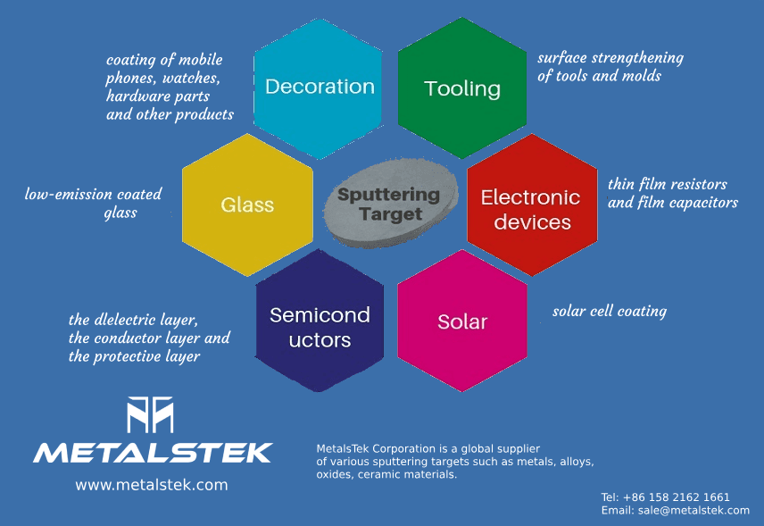
Sputtering targets are used in a wide range of applications, including the production of semiconductors, computer chips, solar cells, low-E glass, optical coatings, and various electronic components.
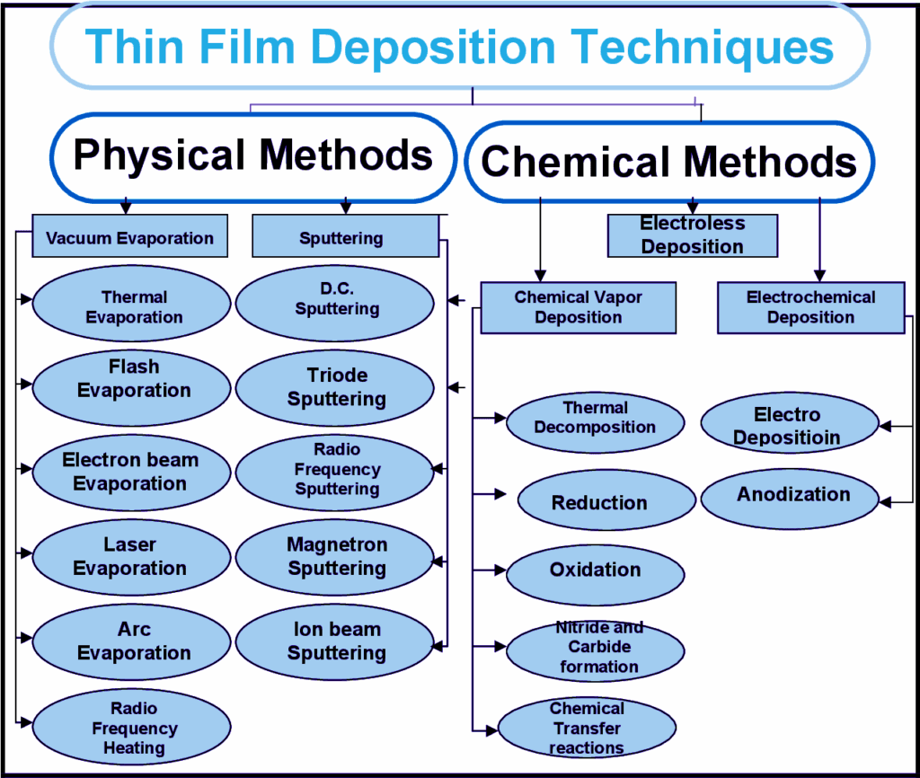
The sputtering process is a physical vapor deposition (PVD) technique used to deposit thin films of materials onto a substrate.
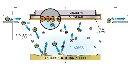
It takes place in a vacuum chamber filled with a low-pressure inert gas, typically argon. A negatively charged target material, known as the sputtering target, is placed in the chamber. A high voltage is applied between the target and the substrate, which causes the inert gas to become ionized, creating a plasma.
The positively charged gas ions in the plasma are accelerated towards the negatively charged target. When these high-energy ions collide with the target, they knock off atoms from the target material. The sputtered atoms from the target travel through the vacuum and deposit onto the substrate, forming a thin film coating.
The sputtering process continues until the desired thickness of the thin film is achieved. The rate of deposition can be controlled by adjusting factors like the power applied, gas pressure, and target material.
Sputtering is used to deposit a wide variety of thin film materials, including metals, alloys, and ceramics, onto substrates for applications in semiconductors, optics, electronics, and more.
The sputtering process can be influenced by various parameters, such as the energy of the ions, the angle of incidence, the target material, and the background gas pressure. Adjusting these parameters can help control the deposition rate, film properties, and overall efficiency of the process.

Sputtering targets are used for a wide range of applications, primarily in the production of thin films through the physical vapor deposition (PVD) process, including:
The sputtering process offers several advantages compared to other thin film deposition techniques, such as:
However, sputtering also has some disadvantages, including:
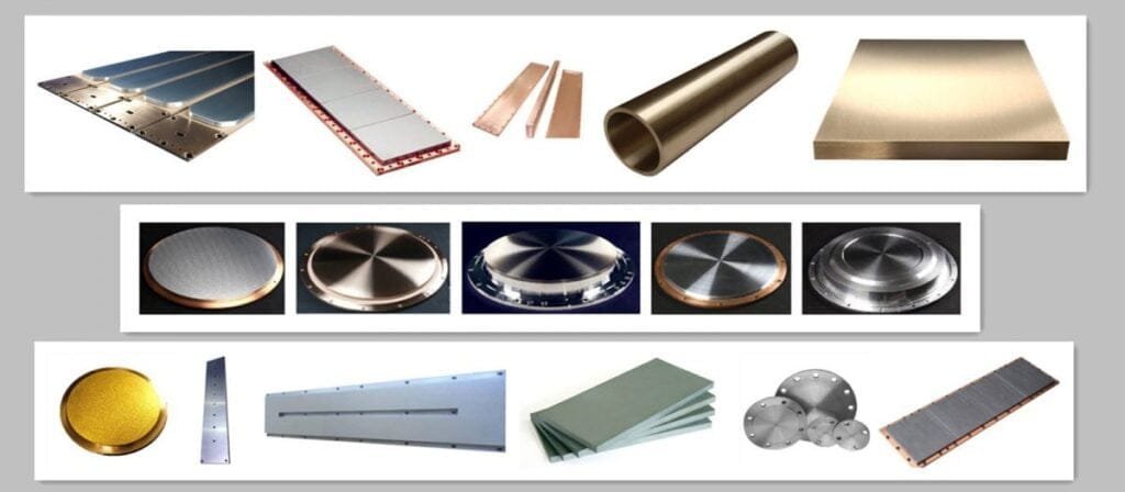
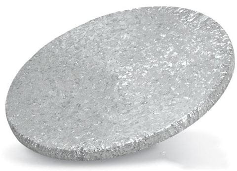
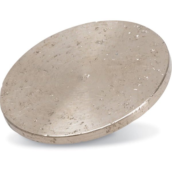
Sputtering targets come in a variety of materials and forms, each suited for specific applications. Some common types of sputtering targets include:
The type of material used for a sputtering target significantly influences the properties and quality of the final thin film. Choosing the right material for a sputtering target depends on the intended application of the thin film, the required properties (e.g., electrical conductivity, hardness, optical properties), and compatibility with the sputtering equipment and process parameters. Each material brings distinct characteristics to the thin films, which can dramatically affect performance in their final application.
Here’s an overview of the common types of materials used for sputtering targets, categorized by their nature and applications:
Sputtering targets not only vary significantly in material composition but also in shape. The shape of a sputtering target can influence the efficiency of the sputtering process, the uniformity of the film deposition, and the overall utilization of the material. Below are the common shapes of sputtering targets used in thin film deposition processes:
Rectangular Targets
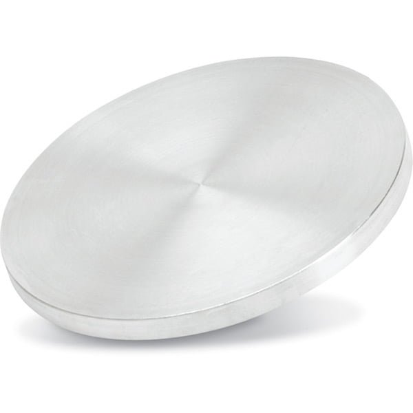
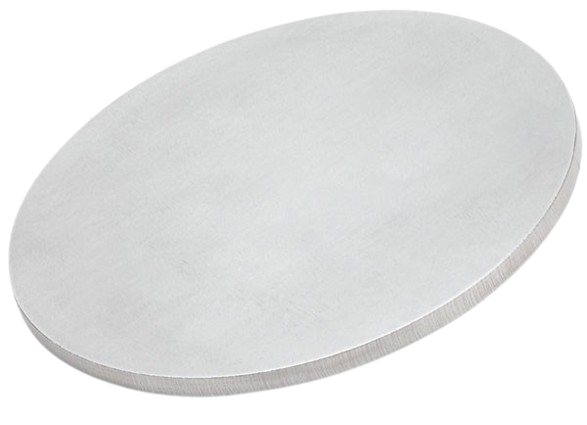
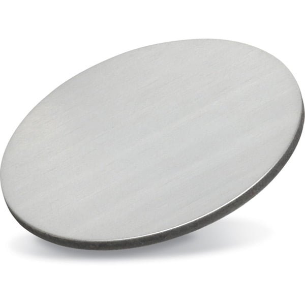
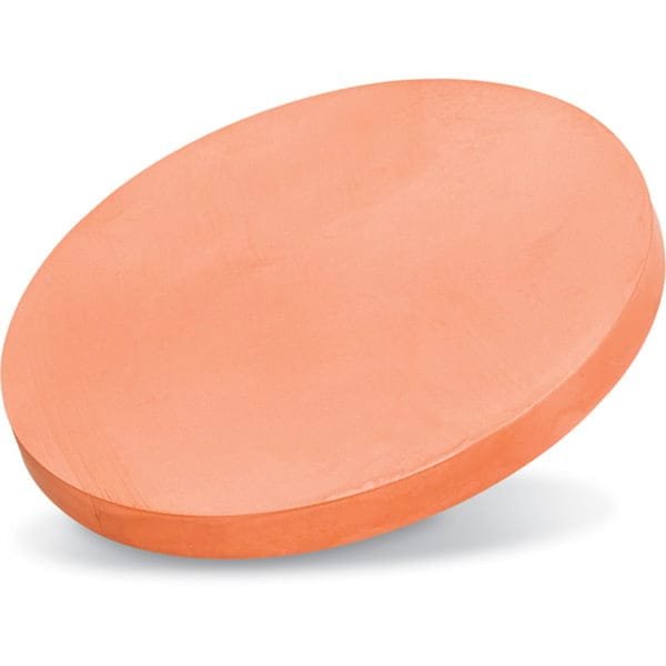
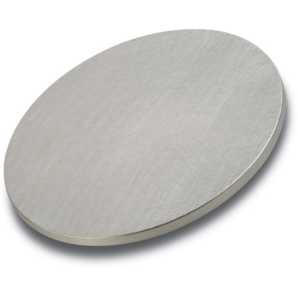
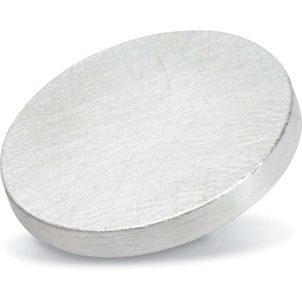
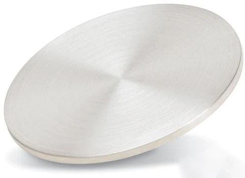
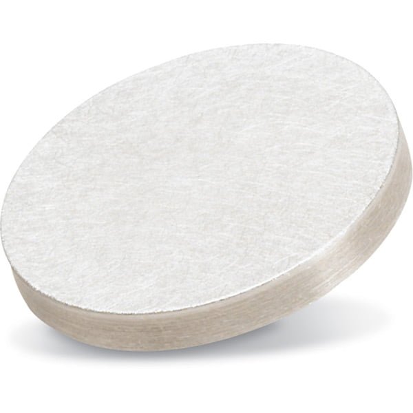
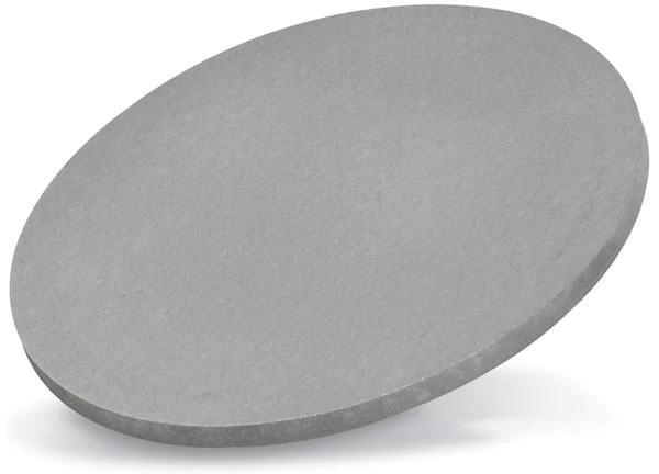
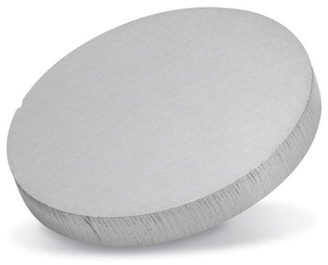
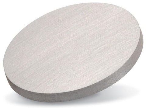
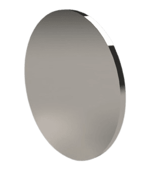
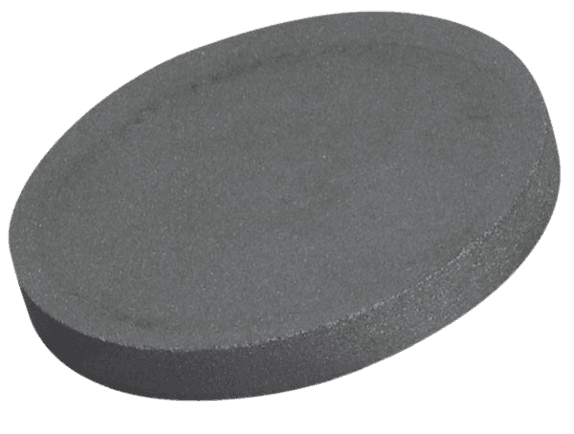
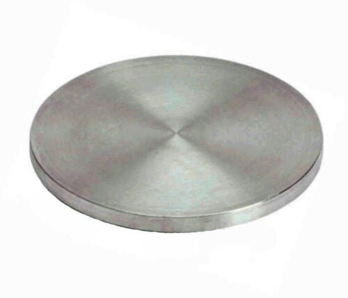
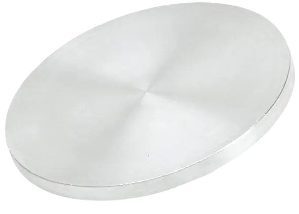
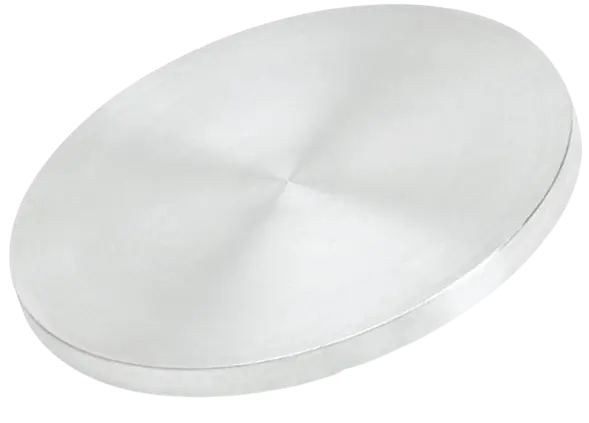
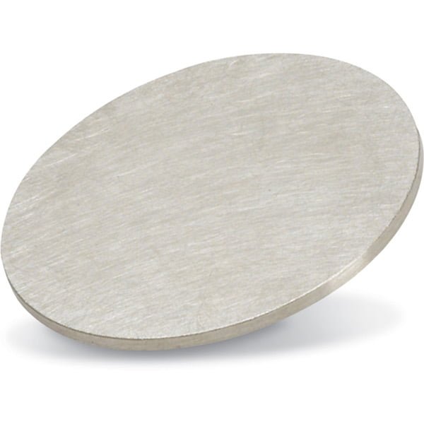
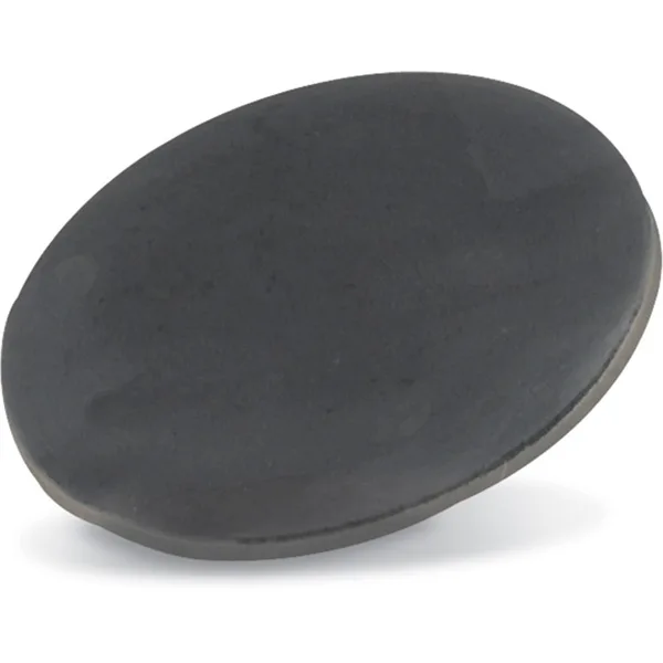
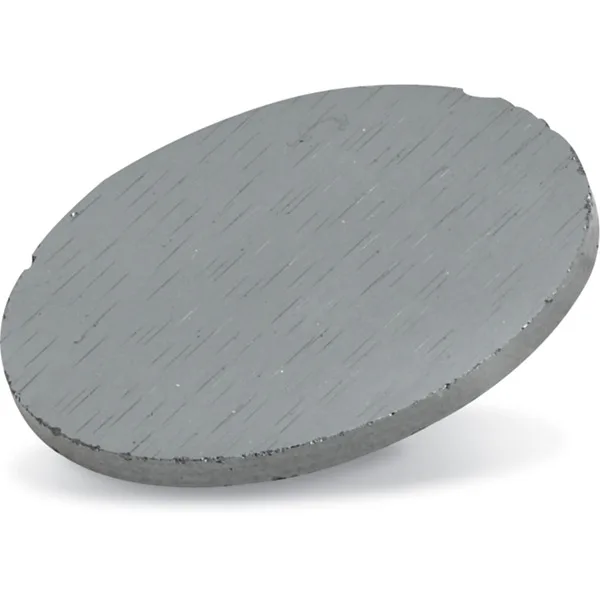
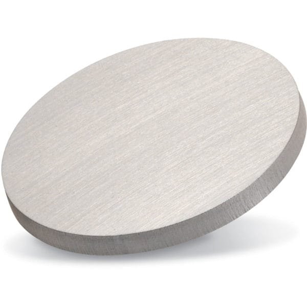
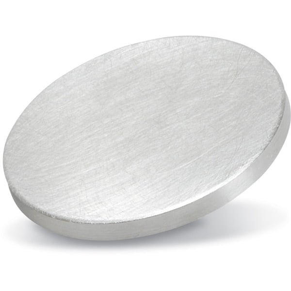
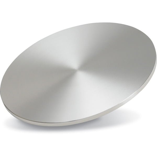
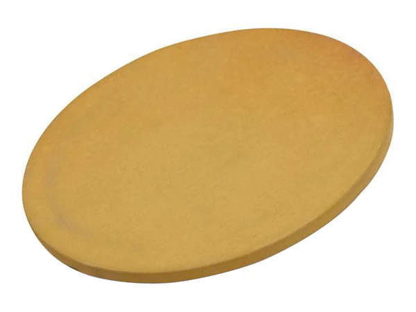
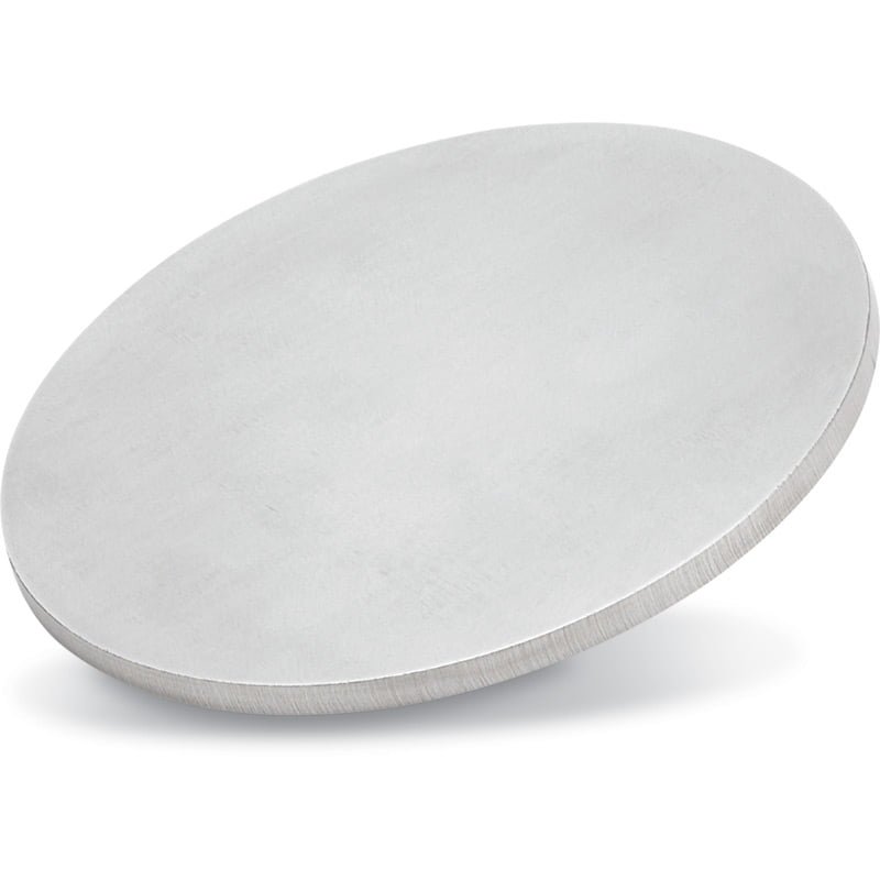
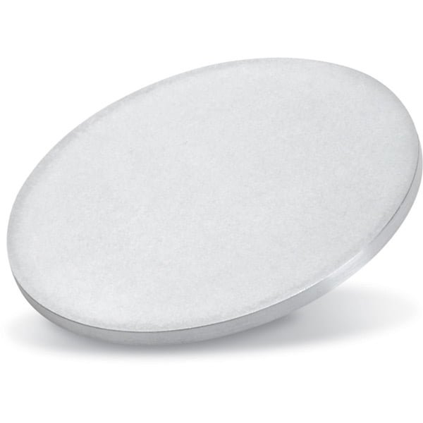
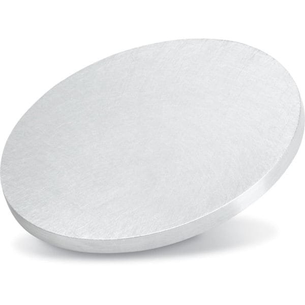
Circular Targets
Rotary Targets
Tube Targets
Ring Targets
Segmented Targets
Considerations for Choosing Target Shapes
The choice of target shape is influenced by several factors:
Target Materials | Pure metal targets Alloy targets Ceramic targets Compound targets (oxides, silicides, carbides, etc.) |
Target Shapes | Planar targets Rotary targets Tubular targets Irregular-shaped targets |
Target Uses | Targets for flat panel displays Targets for semiconductor integrated circuits Targets for solar cell panels Targets for optical components Targets for magneto-optical recording media Targets for automotive coating glass Targets for research purposes Targets for tool coating … |
When choosing sputtering targets, it is important to carefully evaluate the material, mechanical, and operational specifications to ensure they meet the technical requirements of the deposition process and the desired properties of the final thin film. By taking these factors into account, you can improve the performance and cost-effectiveness of the coating process, resulting in better end products.
Sputtering targets are a key component of thin film deposition technologies, which are essential for the progress of electronics, optics, and photovoltaics. Understanding the intricacies of sputtering targets, including their types, applications, and selection criteria, is important in recognizing their significance in advancing modern technology. Whether you work in manufacturing or research, being able to choose the appropriate sputtering target can greatly impact the effectiveness and quality of your thin films. Choose MetalsTek for success.