Introduction
Bismuth Antimony Telluride (Bi/Sb/Te) sputtering targets form the backbone of modern thermoelectric thin-film engineering. With outstanding electrical conductivity, low thermal conductivity, and tunable Seebeck behavior, Bi/Sb/Te alloys have enabled transformative progress in micro-cooling, energy harvesting, infrared detection, and next-generation semiconductor thermal management.
The most widely adopted p-type formulation—Bi₀.₅Sb₁.₅Te₃—continues to lead the field due to its high power factor and stable hole mobility. When deposited via sputtering, this alloy achieves nanoscale film uniformity and optimized crystallographic orientation, giving researchers and device manufacturers unprecedented control over thermoelectric performance.
This article delivers an in-depth exploration of the application scenarios of Bi/Sb/Te sputtering targets, from foundational device physics to cutting-edge commercial and scientific implementations. It also includes authoritative external references for SEO enrichment.
1. Thermoelectric Thin Films: Core Application of Bi/Sb/Te
Thermoelectric thin films convert heat directly into electricity (Seebeck effect) or create cooling using electrical energy (Peltier effect). At the heart of these devices is the precise control of carrier concentration and mobility, which Bi/Sb/Te films are ideally suited for.
1.1 Why Bi/Sb/Te Is the Benchmark Material
- High ZT performance near room temperature
- Low thermal conductivity due to complex crystal structures
- Strong anisotropic behavior beneficial for directional heat management
- Compatibility with RF and DC magnetron sputtering systems
- Ability to form columnar, dense, uniform microstructures
For a broader understanding of thermoelectric fundamentals, readers may consult:
🔗 https://www.sciencedirect.com/topics/engineering/thermoelectric-material (ScienceDirect – Thermoelectric Materials Overview)
1.2 Role in Commercial Thin-Film Modules
Thin-film TE modules built using Bi/Sb/Te are used for:
- Laser diode temperature stabilization
- Sensor cooling
- Precision photonics control
- Micro-electronics thermal management
These applications rely heavily on the quality and stoichiometric precision of sputtered films.
2. Micro-Peltier Coolers for Electronics & Photonics
Micro-Peltier coolers are miniature solid-state cooling devices integrated directly onto chips or optical components. Bi/Sb/Te thin films are essential for achieving stable and rapid heat control in microscale environments.
2.1 Cooling Laser Diodes (LDs)
Laser diodes require temperature stability within ±0.1°C. Even slight fluctuations change:
- Light wavelength
- Output power
- Coherence
Bi/Sb/Te-based micro-coolers are widely used in:
- Fiber-optic communications
- Medical laser systems
- High-power industrial lasers
A useful whitepaper on LD temperature control:
🔗 https://ieeexplore.ieee.org/document/8362158 (IEEE – Laser Diode Thermal Management)
2.2 Infrared Detectors & Imaging Devices
Thermoelectric coolers using Bi/Sb/Te maintain low-noise conditions for:
- Night-vision sensors
- Infrared cameras
- Thermal imaging modules
- Spaceborne detectors
These devices benefit from Bi/Sb/Te’s ability to support rapid, precise, and vibration-free cooling.
3. Energy Harvesting Applications
Bi/Sb/Te sputtering targets play a critical role in thin-film thermoelectric generators (TEGs), designed to convert small temperature differences into usable electrical energy.
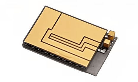
3.1 Wearable Thermoelectric Energy Harvesters
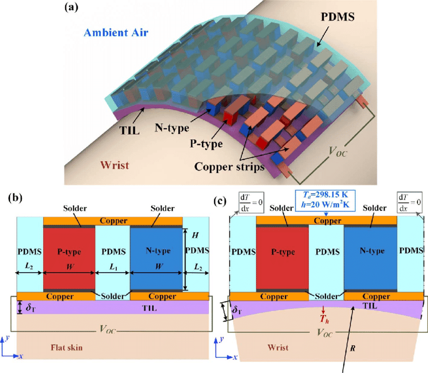
Human-body heat (30–37°C) can be harvested using Bi/Sb/Te films sputtered onto flexible substrates such as:
- Polyimide (PI)
- Polyethylene terephthalate (PET)
- Mica sheets
These films power:
- Health monitoring patches
- Smart textiles
- Mobile medical devices
- Low-power IoT sensors
For more on TE-based energy harvesting:
🔗 https://www.nature.com/articles/nature16050 (Nature – Wearable Thermoelectrics)
3.2 Autonomous IoT Sensors
Internet-of-Things networks often operate in remote, battery-limited environments. TE thin films offer:
- Long-term stable energy supply
- Maintenance-free operation
- Suitability for low-power microelectronics
This is one of the fastest-growing commercial application fields for Bi/Sb/Te thin films.
4. MEMS Thermoelectric Devices
Micro-electromechanical systems (MEMS) increasingly integrate thermoelectric thin films for sensing, thermal regulation, and self-powered functionality.
4.1 TE-MEMS Actuators
Bi/Sb/Te thin films are used to create:
- Thermal actuators
- Micro-resonator stabilizers
- Frequency control modules
Their rapid response time and precise thermal control enable micro-level manipulation.
4.2 On-Chip Thermal Regulation for Silicon Devices
Sputtered Bi/Sb/Te films can be integrated into:
- CMOS wafers
- Silicon photonics
- MEMS gyroscopes
- Microfluidic chips
to stabilize temperature-sensitive elements.
A background reference on MEMS TE devices:
🔗 https://ieeexplore.ieee.org/document/7448411 (IEEE – MEMS Thermoelectric Innovations)
5. High-Performance Sensors & Infrared Technologies
Modern sensor technologies increasingly rely on Bi/Sb/Te thin films for precise thermal control.
5.1 Low-Noise Infrared Sensors
IR sensor sensitivity is strongly temperature-dependent. Bi/Sb/Te micro-coolers:
- Reduce thermal noise
- Improve spectral accuracy
- Enhance signal-to-noise ratios
These properties are essential for:
- Scientific IR detectors
- Gas sensing modules
- Remote environmental detection
5.2 Thermal Cameras & Night Vision Systems
Bi/Sb/Te thin films enable:
- Fast cooling cycles
- Low power consumption
- Compact form factors
- Improved imaging clarity
5.3 Gas and Chemical Sensors
Some modern gas sensors use Bi/Sb/Te films for:
- Localized temperature modulation
- Noise reduction
- Enhanced detection sensitivity
6. Advanced Semiconductor Thermal Management
As semiconductor nodes below 10 nm continue to shrink, thermal management becomes a major reliability challenge.
6.1 Local Hot-Spot Cooling
Bi/Sb/Te thin films cool micro-hotspots on:
- CPUs
- GPUs
- FPGAs
- AI accelerators
Especially for AI workloads, TE micro-cooling offers:
- Highly localized heat handling
- Silent and vibration-free operation
- Integration without moving parts
6.2 Photonics & Optoelectronic Temperature Stabilization
Temperature-sensitive optoelectronic components include:
- VCSELs
- Optical modulators
- Tunable lasers
- Photodetectors
Precise control ensures reliability in demanding applications such as 5G data centers and autonomous driving LiDAR.
7. Flexible Electronics & Next-Generation Wearable Devices
Flexible, lightweight thermoelectric thin films based on Bi/Sb/Te unlock innovations in wearable and bendable electronics.
7.1 Flexible TE Power Films
Sputtered Bi/Sb/Te on PI/PET is used for:
- Body-heat-powered health trackers
- Smart clothing
- Flexible biomedical sensors
7.2 E-Skin (Electronic Skin)
E-skin platforms require:
- Ultra-thin films
- High sensitivity
- Conformal thermal response
Bi/Sb/Te thin films support the thermal sensing layer used in advanced robotics and prosthetics.
A representative reference:
🔗 https://www.sciencedirect.com/science/article/pii/S2542435119301158 (ScienceDirect – Flexible Energy Materials)
8. Space & Aerospace Applications
Space missions require materials that:
- Operate under extreme temperature gradients
- Provide power with no mechanical parts
- Survive radiation exposure
Bi/Sb/Te thin films meet all these requirements, making them suitable for:
- Satellite micro-coolers
- Space sensors
- Deep-space probes
- Thermal stabilization units
9. Research & Development Applications
Bi/Sb/Te sputtering targets are indispensable in research institutions exploring:
9.1 Nanostructured Thermoelectrics
Sputtering enables:
- Superlattice structures
- Nanocomposite films
- Grain-boundary-engineered architectures
All crucial for pushing ZT values beyond conventional limits.
9.2 Material Property Optimization
Researchers adjust:
- Sb content for improved hole mobility (P-type)
- Te/Se ratios for optimized electron conductivity (N-type)
- Deposition parameters to tune:
- Grain size
- Crystal orientation
- Carrier concentration
9.3 High-Throughput Screening
Bi/Sb/Te targets support rapid prototyping via:
- Combinatorial sputtering
- Gradient composition films
- Multi-material co-sputtering
A relevant resource:
🔗 https://www.nature.com/articles/s41598-019-56302-8 (Nature – Thermoelectric Thin-Film Research)
10. Industrial Manufacturing Trends
10.1 Micro-TEG Mass Manufacturing
Industries increasingly use thin-film Bi/Sb/Te to:
- Power remote wireless nodes
- Reduce maintenance in sensors
- Optimize energy collection efficiency
10.2 Automotive Sensors
In EVs and hybrid vehicles, Bi/Sb/Te films help:
- Maintain battery management system temperature
- Improve infrared sensor performance
- Support ADAS and LiDAR components
10.3 Consumer Electronics
Applications include:
- Cooling smartphone camera sensors
- Stabilizing compact laser modules
- Enabling low-power haptic feedback devices
Conclusion
Bismuth Antimony Telluride (Bi/Sb/Te) sputtering targets are among the most strategically valuable materials in modern thermoelectric engineering. Their ability to deliver stable, high-performance thin films underpins innovations in micro-cooling, infrared sensing, energy harvesting, MEMS devices, wearables, and semiconductor thermal management.
From precision photonics to space exploration, Bi/Sb/Te thin films offer unmatched reliability and tunability at the nanoscale. As industries demand tighter temperature control and energy efficiency, the importance of this material system will only continue to grow—making high-purity sputtering targets essential for next-generation research and manufacturing.