
The continued expansion of thin-film photovoltaics, optoelectronics, and high-performance coatings has made multi-component sputtering materials increasingly important to advanced manufacturing. Among these, Copper Indium Gallium (Cu/In/Ga) sputtering targets stand out as a central material for producing CIGS absorber layers, which remain one of the most efficient and versatile semiconductor systems in thin-film solar technology.
This article provides a comprehensive examination of Cu/In/Ga sputtering targets, covering their composition, properties, fabrication methods, performance behavior, industrial use cases, and considerations for equipment integration. The goal is to offer a deep, structured overview beneficial for engineers, procurement specialists, researchers, and production managers seeking reliable and high-performance sputtering materials.
1. Introduction to Copper Indium Gallium Sputtering Targets
Copper (Cu), Indium (In), and Gallium (Ga) form an alloy system that plays an essential role in the creation of the CIGS (Cu(In,Ga)Se₂) absorber material used in thin-film solar cells. Unlike single-element targets, multi-component sputtering materials require rigorous manufacturing control to maintain consistent stoichiometry, density, and microstructure. Because the resulting film’s electronic and optical properties depend heavily on the metal precursor ratio, high-quality Cu/In/Ga targets directly influence device performance.
1.1 The Role of Cu/In/Ga in Thin-Film Coatings
The CIGS process typically involves depositing a metallic precursor layer from a Cu/In/Ga target and subsequently reacting it with selenium or sulfur to form the semiconductor. The metal layer composition determines the final bandgap (typically 1.0–1.7 eV), directly impacting absorption efficiency and cell characteristics.
1.2 Industrial Demand and Relevance
The global thin-film module market continues to evolve, with CIGS offering advantages such as:
- High theoretical efficiency limits
- Superior performance in diffuse or low-light environments
- Flexibility and low weight
- Thermal stability
As a result, the quality and reliability of Cu/In/Ga targets have become critical factors for manufacturers scaling up production.
2. Material Chemistry and Composition
2.1 Typical Elemental Ratios
Cu/In/Ga sputtering targets are generally specified based on atomic ratio ranges such as:
- Cu : (In + Ga) ≈ 0.7 – 1.0
- Ga : (In + Ga) ≈ 0.1 – 0.3
These ratios are designed to achieve desirable semiconductor characteristics after selenization/sulfurization. Manufacturers must maintain precise composition tolerances, typically ±1–2%, to ensure consistent photovoltaic conversion performance.
2.2 Purity Levels
Purity grades commonly range from 3N (99.9%) to 5N (99.999%) depending on application. Higher purity reduces defect formation in the sputtered film, decreases unwanted secondary phases, and enhances electronic transport properties.
2.3 Influence of Metal Composition on Film Behavior
- Copper (Cu): Determines p-type conductivity and influences grain growth.
- Indium (In): Essential for forming the chalcopyrite structure; affects absorber uniformity.
- Gallium (Ga): Adjusts bandgap energy; higher Ga content typically increases cell open-circuit voltage.
Fine-tuning these elements enables manufacturers to balance light absorption, carrier mobility, bandgap level, and thermal stability.
3. Physical and Mechanical Properties
The performance of a sputtering target depends not only on its composition but also on its physical and mechanical integrity.
3.1 Density and Porosity
High-density targets (≥ 98–99% theoretical density) ensure stable sputtering behavior, uniform erosion, and minimized particle generation. Low porosity reduces arcing and improves deposition uniformity.
3.2 Microstructure
A homogeneous microstructure—confirmed by SEM/EDS mapping—helps maintain consistent composition during sputtering. Segregation or clustering can cause non-uniform thin films and device performance issues.
3.3 Electrical and Thermal Conductivity
Because Cu contributes significantly to electrical and thermal properties, the addition of In and Ga modifies the alloy’s conductivity. Proper conductivity ensures efficient sputter plasma coupling and stable power handling.
3.4 Mechanical Strength and Erosion Stability
Targets must withstand thermal stresses from high-power sputtering systems. Proper sintering or casting prevents cracks, delamination, and powder shedding during long production cycles.
4. Manufacturing Processes for Cu/In/Ga Sputtering Targets
Producing a consistent, high-performance Cu/In/Ga target requires specialized knowledge and precision-controlled processes. The most widely used industrial techniques include:
4.1 Powder Metallurgy (PM)
Powder metallurgy is one of the dominant manufacturing routes, especially for complex alloy compositions.
Process steps include:
- High-purity metal powders selection
- Controlled mixing to ensure homogeneity
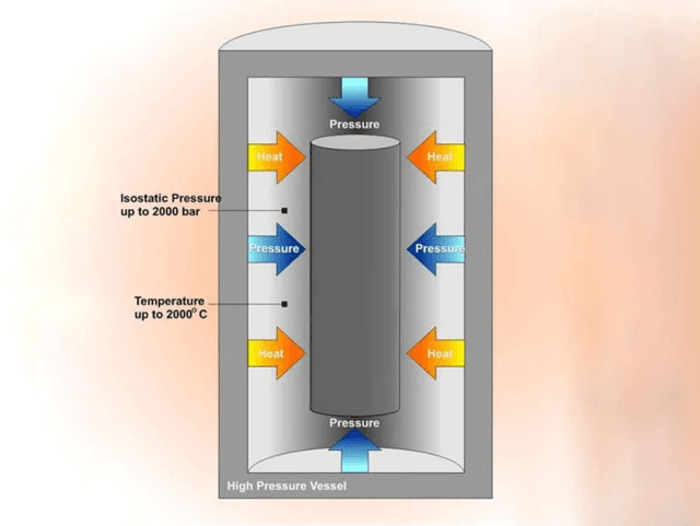
- Cold isostatic pressing (CIP) to form a green compact
- Sintering (usually in vacuum or inert atmosphere)
- Optional hot isostatic pressing (HIP) for additional densification
Advantages:
- Excellent composition control
- High-density targets
- Fine microstructural uniformity
Challenges:
- Requires careful powder preparation
- Higher production cost for ultra-high purity grades
4.2 Vacuum Melting and Casting
Some manufacturers use vacuum induction melting or arc melting to create large, uniform alloy ingots.
Benefits include:
- Good macro-scale homogeneity
- Cost-effectiveness for certain compositions
Limitations:
- More prone to segregation if cooling is not precisely controlled
- May require additional thermomechanical processing
4.3 Hot Pressing
Hot pressing combines heating and pressure to densify the powder. It is appropriate for small and medium-sized targets.
4.4 Bonding to Backing Plates
To improve heat dissipation and prevent warping, targets are often bonded to molybdenum (Mo) or copper (Cu) backing plates through:
- Diffusion bonding
- Indium bonding
- Elastomer bonding (in select systems)
Bonding quality directly affects thermal conductivity, operational stability, and sputtering lifecycle.
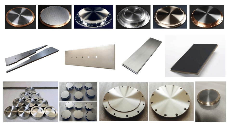
5. Types of Cu/In/Ga Sputtering Targets

Cu/In/Ga targets come in various configurations depending on equipment design and deposition requirements.
5.1 Planar Targets
Commonly used in older or mid-scale deposition systems. Available in rectangular or circular geometries.
5.2 Rotary (Cylindrical) Targets
Rotary targets offer advantages such as:
- Higher target utilization rate (up to 85–90%)
- More uniform film deposition
- Longer continuous operating cycles
These are widely adopted in high-volume photovoltaics manufacturing.
5.3 Custom Dimensions and Segmentation
Some equipment requires segmented or monolithic target designs. Manufacturers often tailor thickness, diameter, bonding type, and material homogeneity according to machine specifications.
6. Sputtering Performance Characteristics
6.1 Deposition Stability
A well-fabricated Cu/In/Ga target provides:
- Consistent sputtering rate
- Lower arcing occurrence
- Reduced particle formation
Stability is one of the most important factors for mass production environments.
6.2 Film Composition Control
Multi-component targets must maintain compositional uniformity across the erosion track to produce consistent thin film stoichiometry. Variations can lead to bandgap inconsistencies across large modules.
6.3 Surface Quality and Target Conditioning
Properly polished surfaces and controlled grain size accelerate target conditioning and reduce ramp-up time during production.
6.4 Target Utilization Efficiency
Factors influencing utilization include:
- Density
- Bonding strength
- Surface flatness
- Cooling efficiency
- Loading geometry within the sputtering chamber
Rotary targets typically achieve the highest usage levels, improving cost-effectiveness.
7. Applications of Cu/In/Ga Sputtering Targets
7.1 CIGS Thin-Film Solar Cell Manufacturing
Cu/In/Ga targets are primarily used to produce the metallic precursor film for CIGS photovoltaic modules. These modules are widely used in:
Utility-scale solar farms
Building-integrated photovoltaics (BIPV)
Flexible and portable solar solutions
Aerospace and specialty electronics due to lightweight design
CIGS remains one of the highest efficiency thin-film technologies, with laboratory efficiencies exceeding 23%.
7.2 Optoelectronic Devices
Thin films derived from Cu/In/Ga targets are used in:
- Photodetectors
- Optical coatings
- Laser materials in experimental systems
7.3 Research and Development
R&D applications include:
- Next-generation tandem solar cell structures
- Thin-film transistors
- Novel semiconductors for flexible electronics
7.4 Energy Storage and Industrial Coatings
Although less common, some researchers utilize Cu–In–Ga alloys for battery interfaces, high-performance metallization layers, and functional coatings due to their tunable electronic behavior.
8. Quality Control, Testing, and Characterization
Ensuring reliable sputtering performance requires comprehensive quality control.
8.1 Chemical and Purity Analysis
- ICP-OES for elemental composition
- GDMS for trace impurities
- XRF mapping for compositional uniformity
8.2 Microstructure Testing
- SEM imaging
- EDS elemental mapping
- Grain size analysis
8.3 Physical Property Measurements
- Density tests (Archimedes method)
- Hardness and mechanical strength
- Thermal conductivity testing
8.4 Bonding Integrity
Ultrasonic C-scan inspection is often used to verify the bond between target and backing plate.
9. Handling, Storage, and Operational Considerations
Even the highest-quality targets require proper handling to maintain performance.
9.1 Storage Guidelines
- Store in dry, clean environments
- Protect against dust and impacts
- Maintain vacuum-sealed packaging until installation
9.2 Pre-Installation Inspection
Technicians should verify:
- Flatness
- Surface integrity
- Bonding condition
- Dimensions compared to equipment specifications
9.3 Conditioning During Initial Operation
Breaking in a target at reduced power can minimize arcing and improve film stability.
9.4 Avoiding Contamination
Contamination from oils, fingerprints, or cleaning agents can affect deposition. Gloves and lint-free handling tools are recommended.
10. Industry Trends and Innovations
10.1 Higher Ga Content Targets
To push CIGS cell efficiency further, some manufacturers explore higher Ga ratios for superior bandgap tuning.
10.2 Larger-Area Deposition
The scaling of photovoltaic manufacturing has driven demand for:
- Wider rotary targets
- Longer planar targets
- Improved target uniformity across large substrates
10.3 Automation and Real-Time Monitoring
Integrated monitoring of erosion profiles and sputtering uniformity leads to improved process control, requiring highly stable target materials.
10.4 Environmental and Recycling Considerations
Recycling indium and gallium from spent targets contributes to sustainability and resource security. Metal recovery programs help reduce material waste.
11. Why High-Quality Cu/In/Ga Targets Matter
Every property of a CIGS absorber—from grain size to charge mobility—is influenced by the metal precursor layer formed from the Cu/In/Ga sputtering target. Therefore:
- Higher uniformity → higher module efficiency
- Better density → longer target life
- Purity control → fewer defects
- Stable erosion → consistent production yield
For industrial users, small improvements in target quality can translate into significant operational savings and efficiency gains.
12. Metalstek’s Capabilities in Cu/In/Ga Target Production
Metalstek specializes in precision-engineered sputtering materials designed for both R&D and large-scale manufacturing.
Key advantages include:
- High-purity raw materials
- Advanced powder metallurgy and vacuum melting capabilities
- Customized compositions and geometries
- High-density, low-porosity microstructures
- Strong bonding to Mo and Cu backing plates
- Consistent quality control and documentation
- Responsive technical support
Whether for photovoltaics, semiconductors, or research, Metalstek delivers reliable Cu/In/Ga materials optimized for stable sputtering and high-yield production.
Conclusion
Copper Indium Gallium sputtering targets are integral to one of the most advanced thin-film deposition processes in the modern energy and electronics industries. Their complex alloy composition, demanding fabrication requirements, and direct influence on device performance make them a premium material that requires precision engineering.
High-quality Cu/In/Ga targets ensure:
- Efficient, uniform film deposition
- Reliable CIGS absorber formation
- Stable manufacturing processes
- Long-term device performance and durability
As the demand for durable, flexible, and high-efficiency renewable technologies expands, Cu/In/Ga targets will continue to play a pivotal role in shaping the future of thin-film materials and photovoltaic production.