
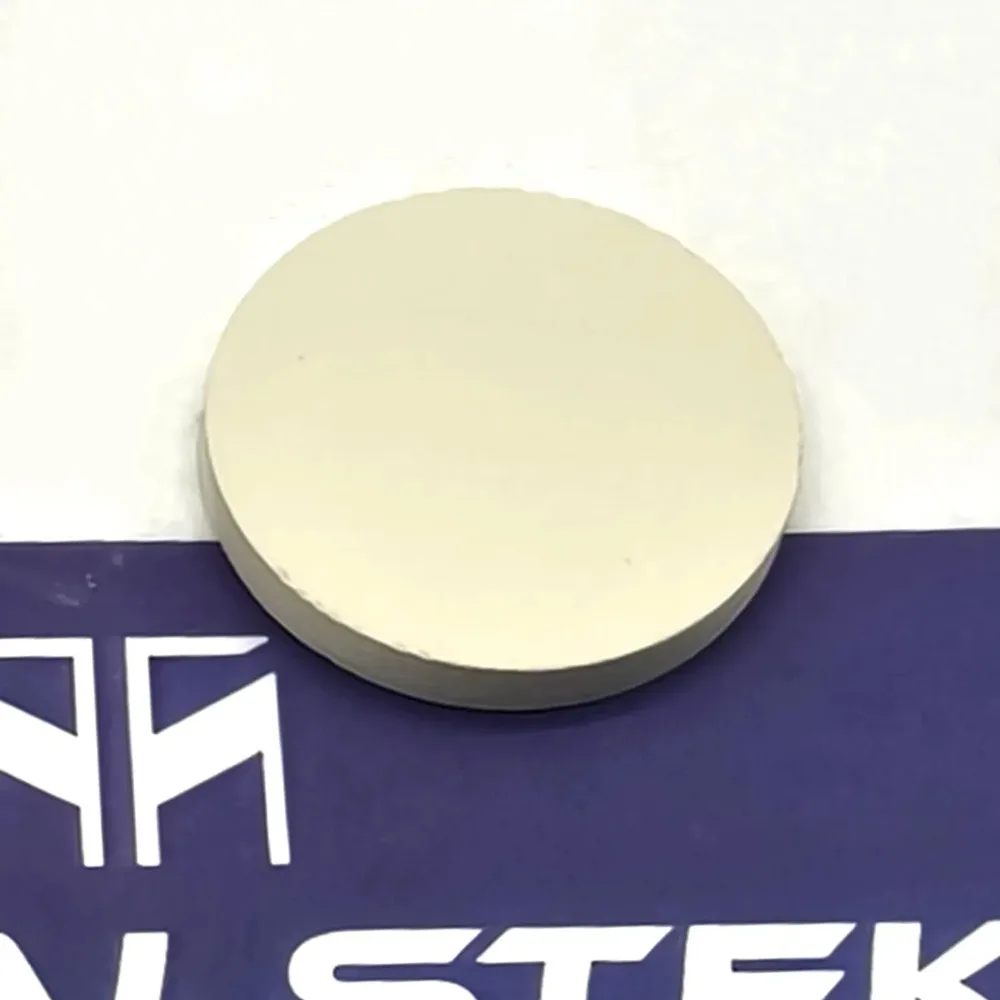
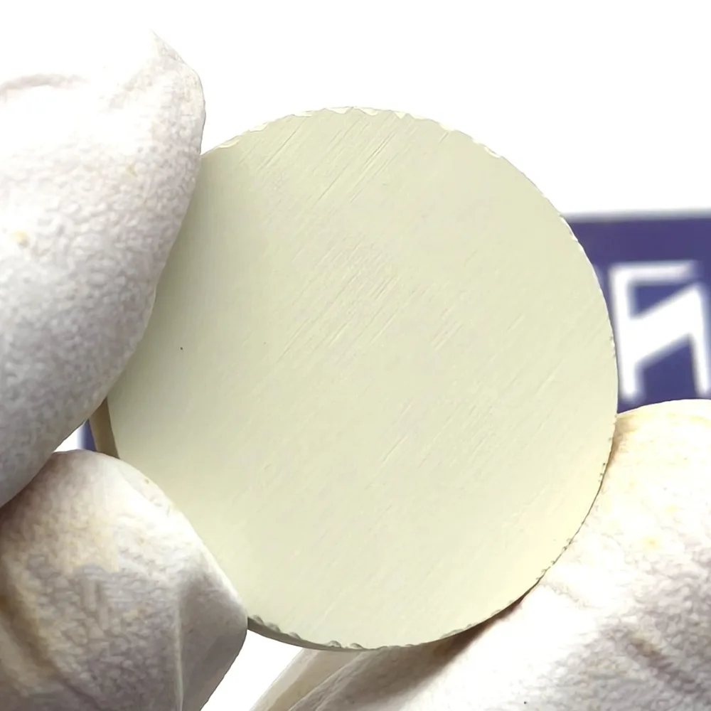
Gallium Nitride (GaN) is one of the most critical materials in advanced semiconductor and optoelectronic technologies. If you need a sputtering target that delivers uniformity, purity, and stable performance in deposition, you’re in the right place. MetalsTek provides precision-engineered GaN sputtering targets with customizable specifications, ideal for power electronics, LEDs, laser diodes, UV detectors, and high-frequency transistors.
Our GaN targets are designed to meet the demanding requirements of R&D labs, semiconductor fabs, and thin-film coating applications. With high purity levels (typically 99.9% to 99.999%), exceptional structural integrity, and support for multiple bonding options, we ensure performance that meets the most critical process needs.
Key Features of MetalsTek GaN Sputtering Targets
- Purity Options: 99.9% (3N), 99.99% (4N), and 99.999% (5N) available based on your process and end-use requirements.
- Custom Dimensions: Diameters from 1” to 12” or larger; thicknesses starting at 1 mm; rectangular or annular shapes also supported.
- Bonding Support: Indium, elastomeric bonding, or direct mount options available with Cu, Mo, or other backing plates.
- Density & Microstructure: Fully densified, fine-grain targets ensure minimal particle generation and uniform thin-film growth.
- Packaging: Targets are vacuum-sealed in inert atmosphere, protected from oxidation and physical damage during shipment.
Common Applications
- Thin-film deposition for GaN-on-Si and GaN-on-Sapphire devices
- Blue and UV LEDs, laser diodes, and photodetectors
- High electron mobility transistors (HEMTs) and RF power amplifiers
- Optical and protective coatings in aerospace, telecom, and military electronics
- R&D for next-gen power switching and quantum computing hardware
Target Specifications
| Feature | Range / Detail |
|---|---|
| Purity | 99.9% – 99.999% |
| Sizes | Ø25 mm to Ø300 mm, or custom |
| Shape Options | Round, rectangular, annular |
| Bonding | Indium, elastomer, or unbonded |
| Backing Plates | Cu, Mo, W, custom alloys |
| Packaging | Vacuum sealed, moisture-free |
Let’s Talk Specs
Need a specific size, purity, or bonding configuration? We’ve delivered GaN targets to clients in semiconductor research, optoelectronics manufacturing, and defense. Tell us what you’re working on — we’ll respond with a tailored solution and fast quote.
You May Also Want to Know
1. What is a GaN sputtering target?
A GaN sputtering target is a solid source of gallium nitride used in physical vapor deposition systems. Under plasma bombardment, it releases Ga and N atoms that deposit onto a substrate, forming a thin film.
2. What purity levels are available for GaN targets?
GaN sputtering targets are available in 99.9%, 99.99%, and ultra-high-purity 99.999% grades depending on film quality and device requirements.
3. Which shapes and sizes can GaN targets be made in?
GaN targets can be supplied in round, rectangular, or custom shapes, with diameters ranging from 1 inch to 12 inches and thicknesses from 1 mm upward.
4. Why are backing plates used for GaN targets?
Backing plates improve heat transfer and mechanical stability during sputtering. GaN is brittle, so bonding it to copper or molybdenum backing plates helps prevent cracking and improves process reliability.
5. What are the thermal and physical properties relevant to GaN sputtering?
GaN has a high melting point (~2500°C), excellent thermal conductivity, and a wide bandgap (3.4 eV). These properties make it ideal for high-power and high-frequency electronics.
6. What deposition methods are suitable for GaN targets?
GaN targets are typically used in RF magnetron sputtering systems due to their semi-insulating nature. Some setups also support pulsed DC sputtering for GaN.
7. How does target quality influence film uniformity and defects?
Higher density and low impurity targets produce fewer particles, enable uniform erosion, and result in smoother, defect-free thin films.
8. What applications use sputtered GaN films?
Applications include microLEDs, RF transistors, blue lasers, UV sensors, and high-frequency power devices.
9. How should GaN targets be handled and stored?
Store in original vacuum packaging until ready for use. Handle with clean gloves to avoid contamination. Avoid mechanical shock due to brittleness.
10. What is the ramp-up/ramp-down best practice for GaN targets?
Use gradual power increases to prevent thermal shock or bonding failure. Maintain uniform cooling during operation to minimize stress.
11. What typical lead times apply for custom GaN targets?
Lead times range from 2 to 6 weeks depending on shape, size, bonding, and purity requirements.
12. Can GaN targets be doped or alloyed?
Yes. GaN targets can be doped with elements such as Si or Mg for specialized optoelectronic or semiconductor properties.
13. How is GaN target purity verified?
Analytical methods like glow discharge mass spectrometry (GDMS) or X-ray fluorescence (XRF) are used to ensure material purity.
14. What are common failure modes for GaN targets?
Cracking, delamination from backing plates, particle shedding, and non-uniform erosion are common issues when improperly handled.
15. Can clients bond their own GaN target to backing plates?
Yes, but it requires precise technique and thermal matching. Improper bonding can result in poor thermal contact or target damage.
16. What packaging and shipping considerations exist for GaN targets?
They are vacuum-sealed in protective film, then packed with cushioning inside anti-static or custom-fit containers to avoid moisture and impact.
17. Is GaN reactive or hazardous under certain conditions?
While GaN is generally stable, it can be damaged by moisture and should not be exposed to acids or high humidity. Powders require additional handling care.
18. Can GaN oxide (e.g. GaOxN) sputtering targets be used instead?
Yes, oxide variants of GaN can be used for specialized dielectric or optical coatings but require different deposition parameters.
19. How to mitigate target poisoning in GaN sputtering?
To avoid target poisoning, control the partial pressure of reactive gases and ensure a clean, well-conditioned target surface.
20. What safety or handling precautions should be used when working with GaN targets?
Use standard lab safety protocols, wear gloves, avoid sudden temperature changes, and follow handling guides to preserve material integrity.