Looking for premium erbium sputtering targets for your thin-film or photonic device projects? MetalsTek offers high‑purity erbium (Er) targets with tailored dimensions, backed by strict quality control and fast quotes.
Why Choose Our Erbium Sputtering Targets?
- Purity & performance: We offer Er targets in purity grades from 99.9 % up to 5N (99.999 %) to satisfy demanding optical, telecom, and research applications.
- Optimized physical properties: Theoretical density ~9.07 g/cm³, melting point ~1,529 °C, thermal conductivity ~15 W/m·K – ideal for stable sputtering performance.
- Flexible shapes & backing options: Discs, rectangles, annular shapes, bonded or unbonded, with backing plates (Cu, Mo, etc.) for better heat sinking.
- Low defect & uniform film growth: Our processing ensures fine grain size, high density, and minimal inclusions to deliver low particle generation and consistent film uniformity.
Typical Specs & Custom Options
| Parameter | Typical Value / Range | Notes |
|---|---|---|
| Purity | 99.9 % to 99.999 % | Depending on applications |
| Dimensions | Ø 25 mm – 200 mm (or custom) | Thickness from 1 mm upward |
| Bonding | Indium, elastomer, direct | Based on sputtering power & cooling needs |
| Packaging | Vacuum sealed, inert gas | To prevent oxidation during shipping |
Applications & Use Cases
- Photonics & optical coatings: Because erbium has a sharp optical emission (especially around 1.54 µm), it’s widely used in waveguides, amplifiers, and optical filters.
- Telecom & fiber optics: Er-doped layers are integral in optical amplifiers and rare-earth-doped fiber amplifiers (EDFAs).
- Thin-film research & R&D: Suited for magnetron sputtering, ion-beam sputtering, and multi-layer deposition systems.
- Specialty coatings & quantum devices: For integrated photonics, sensors, and laser systems requiring high purity rare earths.
Why MetalsTek?
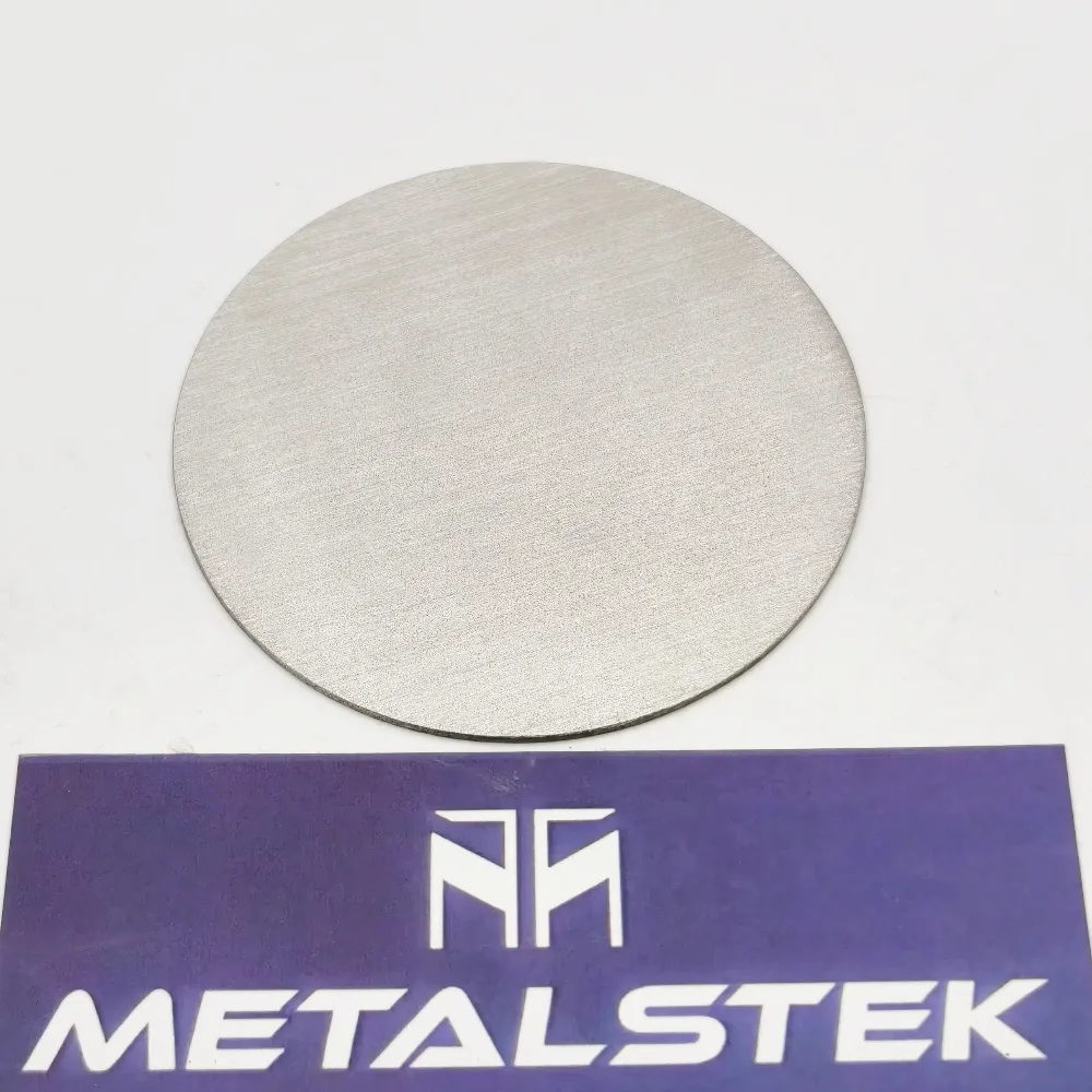
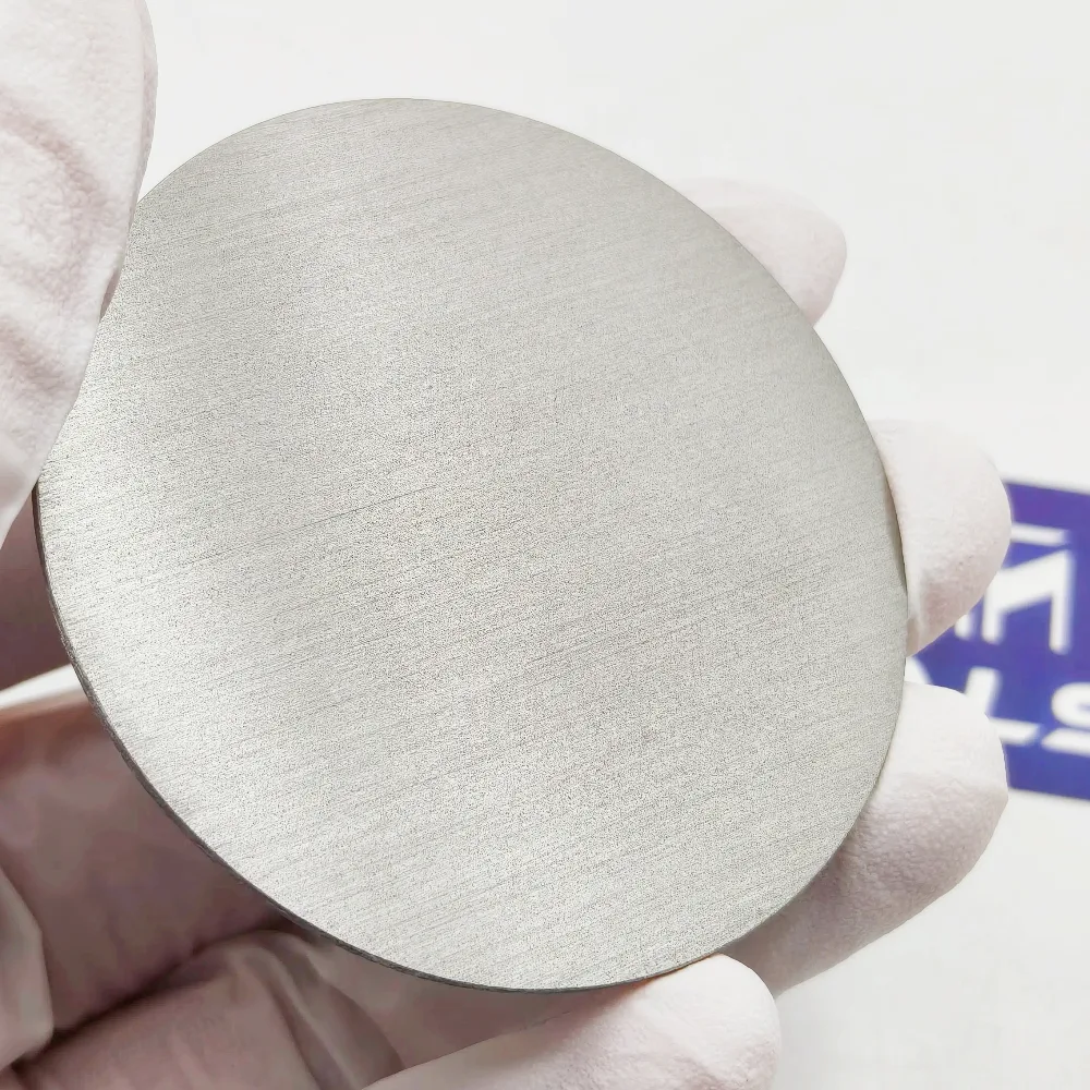
At MetalsTek, we understand that not every product gets a standalone page—but every product deserves precision, trust, and responsiveness. When you browse our gallery, you’ll see real photos (as above) illustrating surface finish, bonding quality, and dimensions. Pair that with accurate specs and a fast quote, and you’ve got a reliable partner.
Explore the photo gallery above and request a quote today. Tell us your required purity, dimensions, backing preferences, or application — we’ll get back within 1 business day.
You May Also Want to Know
1. What is an erbium sputtering target?
An erbium sputtering target is a high-purity source material made of erbium metal, shaped for use in sputter deposition systems. When bombarded with ions, it releases atoms that coat a substrate with a thin film.
2. What purity grades are available for erbium sputtering targets?
Common purity levels range from 99.9% (3N) to 99.999% (5N), depending on the quality requirements of the optical or electronic applications.
3. Which shapes and sizes can erbium sputtering targets be manufactured in?
They are available in disc, rectangular, annular, and step target formats. Sizes typically range from 1 inch to 8 inches in diameter, with thicknesses from 1 mm and up.
4. What backing or bonding methods are used for erbium targets?
Erbium targets may be bonded to copper or molybdenum backing plates using indium bonding or elastomeric materials for better thermal management and mechanical strength.
5. What are the thermal and physical properties of erbium relevant to sputtering?
Erbium has a melting point of 1,529°C, a density of 9.07 g/cm³, and thermal conductivity around 15 W/m·K. These properties affect how it behaves during sputtering.
6. What power density is recommended when sputtering erbium?
A typical starting point is around 20 watts per square inch, but this may vary depending on the bonding, system configuration, and cooling efficiency.
7. Which deposition methods are compatible with erbium sputtering targets?
Erbium targets can be used in DC magnetron sputtering, RF sputtering, and pulsed sputtering systems depending on the equipment and film requirements.
8. How does the target quality affect film uniformity and defects?
Higher density and low impurity targets reduce particle generation and improve film adhesion, thickness uniformity, and optical clarity.
9. What are typical applications for erbium-based sputtered films?
They are used in optical amplifiers, waveguides, lasers, filters, and photonic devices, especially in the telecom and IR optics industries.
10. How should one handle or store erbium sputtering targets to preserve quality?
They should be stored in vacuum-sealed or inert-gas packaging, handled with gloves or clean tools, and kept away from moisture and contaminants.
11. What is the recommended ramp-up and ramp-down procedure for Er or Er₂O₃ targets?
Always start with a slow power ramp to reduce thermal stress and avoid cracking or delamination, especially with bonded or ceramic targets.
12. How long does it typically take to custom-produce an erbium sputtering target?
Standard sizes may be ready to ship within 2–4 weeks, while custom targets may require 4–8 weeks depending on the complexity and quantity.
13. Can erbium targets be alloyed or doped for special applications?
Yes, erbium can be combined with other elements for specific optical or electrical characteristics. These custom alloys are often used in R&D.
14. How is the purity of an erbium target verified or certified?
Analytical techniques such as GDMS or ICP-MS are used to confirm elemental purity and trace impurity levels.
15. What are common failure modes of erbium sputtering targets?
Failures include bonding separation, cracking due to thermal stress, arcing from surface defects, or non-uniform erosion during long runs.
16. Can customers bond their own erbium targets to backing plates?
Yes, but correct technique and thermal matching are essential. Poor bonding can cause thermal failure or sputter instability.
17. What packaging and shipping considerations apply to erbium targets?
They are usually vacuum-sealed in anti-static or inert packaging and cushioned against vibration to prevent oxidation or mechanical damage.
18. Is erbium metal reactive or hazardous?
Erbium is relatively stable but should still be handled under clean, dry conditions. Fine powders may oxidize faster and require special handling.
19. Can an erbium oxide (Er₂O₃) sputtering target be used instead of metal Er?
Yes, if the desired film is an oxide. Er₂O₃ targets are common in dielectric and optical applications, though sputtering conditions differ.
20. What safety or handling precautions should be considered during use?
Always use clean handling tools, follow SDS guidelines, and operate sputtering equipment within recommended parameters to avoid damage or contamination.