Introduction
Niobium nitride (NbN) is one of the most influential transition-metal nitrides used in modern thin-film technology. Known for its high superconducting transition temperature (Tc ≈ 16 K), superior hardness, excellent chemical stability, and metallic conductivity, NbN plays a critical role in next-generation electronics, photonics, quantum devices, and protective coatings.
As a sputtering target, NbN enables the controlled deposition of dense, uniform, and phase-pure NbN thin films through magnetron sputtering or reactive sputtering (Nb + N₂ plasma). With tunable stoichiometry and multiple crystalline phases—including δ-NbN, γ-Nb₂N, and Nb₄N₅—the material offers versatile properties tailored to superconducting circuits, barrier layers, IR detectors, and wear-resistant coatings.
This long-form guide provides an in-depth exploration of NbN sputtering targets, covering their material structure, deposition behavior, manufacturing technologies, and real-world applications across semiconductor fabrication, cryogenic electronics, and optical systems.
1. Material Overview of Niobium Nitride (NbN)

1.1 Crystal Chemistry and Phase Formation
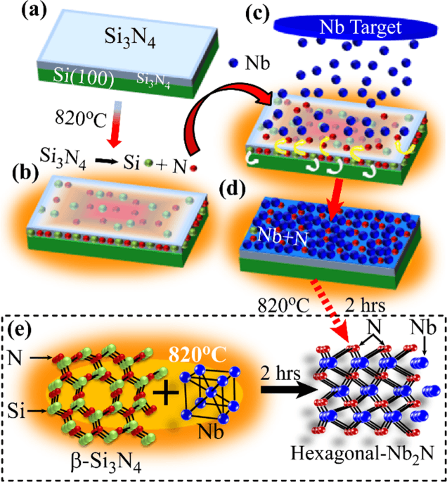
NbN belongs to the family of rock-salt structure transition metal nitrides, exhibiting a face-centered cubic (FCC) lattice similar to TiN and VN. However, unlike many group V nitrides, NbN exhibits several metastable phases depending on deposition conditions:
- δ-NbN (cubic) – superconducting phase, metallic, widely used
- γ-Nb₂N (hexagonal) – harder but lower superconducting properties
- δ′-NbN (tetragonal) – intermediate stability
- Nb₄N₅ (orthorhombic or monoclinic) – nitrogen-rich, high resistivity
The ability to tune phase content through sputtering parameters gives NbN coatings an exceptional property-to-performance adjustability.
1.2 Key Physical and Chemical Properties
| Property | Typical Value | Significance |
|---|---|---|
| Crystal Structure | Cubic (δ-NbN) | Preferred for superconductivity |
| Superconducting Tc | 15–16 K | Enables quantum and cryogenic electronics |
| Electrical Resistivity | 80–250 µΩ·cm (film-dependent) | Wide tunability via stoichiometry |
| Hardness | 20–25 GPa | Suitable for protective coatings |
| Optical Behavior | Strong IR absorption, adjustable reflectivity | IR sensors and filtering applications |
| Chemical Stability | High | Resists corrosion, oxidation under moderate temperatures |
| Melting Point | ~2573 °C | High-temperature stability |
These intrinsic characteristics are the foundation of NbN’s relevance in advanced thin-film technologies.
2. NbN Sputtering Target Manufacturing and Material Quality

Producing high-performance NbN films begins with a well-engineered sputtering target. Manufacturing routes strongly influence microstructure, density, and purity.
2.1 Raw Material Selection
NbN sputtering targets typically start from:
- High-purity niobium metal (99.95%–99.99%)
- High-purity nitrogen gas or pre-synthesized NbN powders
- Controlled oxygen (<100 ppm), carbon (<200 ppm), and metallic impurity levels
Purity is directly linked to superconducting and electrical film performance.
2.2 Target Fabrication Techniques
(a) Solid-State Reaction + Hot Pressing
A stoichiometric mixture of Nb and N₂ is reacted and hot-pressed at high temperature to form a dense NbN ceramic.
- Density: >98% theoretical
- Grain size: 1–10 µm
(b) Cold-Isostatic Pressing (CIP) + Sintering
NbN powder is compacted under isostatic pressure and sintered.
- Lower cost
- Moderate density
- Suitable for general coatings
(c) Hot Isostatic Pressing (HIP)
Produces near-defect-free NbN targets for demanding superconducting applications.
- High density
- Excellent mechanical stability
(d) Plasma Spheroidization (for powder feedstock)
Used for custom targets requiring special microstructure.
2.3 Backing Plate Options
For planar magnetron sputtering, NbN targets may be:
- Unbonded (solid ceramic)
- Indium-bonded
- Elastomer-bonded
- Copper backing plates for heat removal
- Titanium or Mo backing for thermal expansion matching
The bonding method influences thermal conductivity, stress tolerance, and sputtering stability, especially during long deposition cycles.
3. Deposition of NbN Thin Films
3.1 Sputtering Methods
Niobium nitride films can be produced by:
(a) Direct NbN Sputtering
Using a stoichiometric NbN ceramic target in:
- DC magnetron sputtering
- RF magnetron sputtering
- Pulsed DC sputtering
Advantages:
- Stable stoichiometry
- Uniform composition
- Ideal for superconducting circuits
(b) Reactive Sputtering of Nb Metal with Nitrogen
Sputtering pure niobium in an Ar + N₂ mixture.
Advantages:
- Flexible nitrogen control
- Ability to explore multi-phase regions
- Good for protective and optical coatings
Trade-off: Nitrogen flow instability may cause hysteresis behavior.
3.2 Parameters Influencing Film Properties
| Parameter | Effect on Film |
|---|---|
| N₂/Ar ratio | Controls stoichiometry, phase composition (NbN vs Nb₂N) |
| Substrate temperature | Improves crystallinity; affects Tc and hardness |
| Bias voltage | Controls film density and stress |
| Sputtering power | Influences grain size and deposition rate |
| Pressure | Alters microstructure and optical properties |
NbN is highly tunable. For example:
- Higher N₂ flow → higher resistivity, improved optical absorption
- Higher substrate temperature (>400 °C) → larger grains, better superconducting performance
- Substrate biasing → denser coatings, lower pin-hole density
3.3 Microstructure Evolution
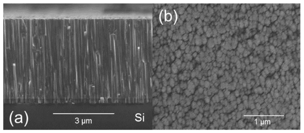
NbN coatings may exhibit:
- Columnar grains (low-T deposition)
- Dense nanocrystalline structure (with bias)
- Epitaxial growth on sapphire, MgO, or SiC
Microstructure strongly correlates with superconductivity, hardness, and optical constants.
4. Superconducting Applications of NbN Films
4.1 Superconducting Nanowire Single-Photon Detectors (SNSPD)
NbN is the industry-standard material for SNSPDs because of:
- High Tc (~16 K)
- Fast response
- High critical current density
- Excellent sensitivity in infrared wavelengths (1–5 µm)
SNSPDs enable:
- Quantum communication
- LiDAR
- Deep-space optical communication
- Ultrafast spectroscopy
4.2 Josephson Junctions and Superconducting Circuits
NbN thin films are widely used in:
- Superconducting quantum bits (qubits)
- Rapid single flux quantum (RSFQ) logic circuits
- THz detectors
Advantages:
- Higher operating temperature than Nb (Tc ~9 K)
- Better noise performance
- Chemically stable in fabrication processes
4.3 Microwave Kinetic Inductance Detectors (MKIDs)
NbN films demonstrate excellent frequency response for:
- Astronomy (sub-mm and far-IR detection)
- Cryogenic sensors
- Low-signal RF systems
4.4 Superconducting Transmission Lines
Used in cryogenic computing hardware, enabling:
- Low-loss signal routing
- Reduced heat dissipation
- Improved quantum system coherence
5. Semiconductor and Electronic Applications
5.1 Diffusion Barrier for Copper Metallization
NbN is an effective Cu diffusion barrier, offering:
- Thermal stability at >600 °C
- Resistance to copper penetration
- Strong adhesion to dielectrics and metals
Used in:
- Interconnects
- TSVs (through-silicon vias)
- MEMS devices
5.2 Gate Electrodes and Conductive Layers
NbN can serve as:
- A stable high-temperature gate electrode
- A metallic layer with good conductivity
- A buffer layer for epitaxial nitrides (AlN, GaN, etc.)
5.3 IR Sensors and Optical Thin Films
NbN has strong infrared absorption, making it useful in:
- Thermal imaging sensors
- IR shielding films
- Optical filters
Optical constants can be tuned by adjusting nitrogen flow during sputtering.
6. Mechanical, Wear, and Decorative Coatings
Transition metal nitrides are widely used for protective coatings. NbN offers:
- High hardness (20–25 GPa)
- Good wear resistance
- Low friction
- Chemical inertness
6.1 Cutting Tools and Forming Tools
NbN coatings provide:
- Improved tool life
- Heat resistance during machining
- Oxidation resistance
Useful for:
- Drills, milling tools
- Forming dies
- High-load mechanical parts
6.2 Biomedical Instrumentation
Because NbN is biocompatible and corrosion-resistant, it sees use in:
- Dental tools
- Surgical instruments
- Implants (as a thin protective layer)
6.3 Decorative Coatings
NbN can produce unique colors—ranging from metallic gray to golden tints—depending on nitrogen content, useful for:
- Watches
- Jewelry
- Consumer electronics housings
7. Optical and Photonic Applications
7.1 Tunable Optical Constants
Film refractive index (n) and extinction coefficient (k) vary with:
- Phase composition
- Nitrogen content
- Deposition energy
This allows NbN to be engineered for:
- Optical absorbers
- Plasmonic devices
- Anti-reflection coatings
7.2 Fabry–Pérot Interference Layers
With stable metallic behavior, NbN can be used in multilayer stacks, particularly in IR optical coatings.
7.3 Hot-Electron Photodetectors
NbN’s electronic structure makes it suitable for ultrafast hot-electron devices.
8. Technical Parameters of NbN Sputtering Target
| Parameter | Typical Value / Range | Importance |
|---|---|---|
| Purity | 99.5% – 99.99% | Affects resistivity and Tc |
| Density | ≥ 95% theoretical | Reduces arcing and improves film uniformity |
| Composition | Nb:N = 1:1 (stoichiometric) | Ensures proper superconductivity |
| Target Type | Planar / Rotary | Flexible for R&D or mass production |
| Size | Custom: Ø25–300 mm, up to 6–12 mm thick | Matches magnetron systems |
| Backing | Cu, Ti, Mo, indium-bonded | Enhances heat transfer |
9. Comparison with Other Transition Metal Nitrides
| Material | Key Advantage | Typical Application |
|---|---|---|
| NbN | Best superconducting performance among nitrides | SNSPDs, quantum devices |
| TiN | Cost-effective, golden color | Hard coatings, decorative |
| TaN | Superior diffusion barrier | IC metallization |
| ZrN | High hardness, yellow-gold appearance | Cutting tools, decorative |
| VN | Conductive, good hardness | Wear coatings |
NbN stands out for its superconducting and electronic behavior.
10. Quality Control and Characterization
10.1 Target Quality Testing
- Density measurement
- XRD phase verification
- Impurity analysis (ICP-MS, GDMS)
- Ultrasound scanning for voids
- SEM for microstructure
10.2 Thin-Film Characterization
- TEM for nanostructure analysis
- XPS for oxidation and stoichiometry
- AFM for surface roughness
- Electrical resistivity vs. temperature
- Critical temperature (Tc) measurement for superconducting films
11. Common Challenges in NbN Deposition
11.1 Reactive Sputtering Instability
Nitrogen hysteresis leads to difficulty maintaining stoichiometry. Using a pre-synthesized NbN target solves this.
11.2 Film Stress and Cracking
High internal stress may require:
- Substrate heating
- Adjusted biasing
- Multilayer design
11.3 Phase Mixing
Too much nitrogen produces Nb₄N₅; too little produces Nb₂N. Careful process control is essential.
12. Packaging, Handling, and Storage
NbN targets are ceramic-like and require careful packaging:
- Vacuum-sealed or inert gas packaging
- Shock-absorbing foam
- Wooden or carton export-safe crates
- Clear labeling for traceability
Conclusion
Niobium nitride sputtering targets enable a vast spectrum of advanced thin-film applications—from superconducting quantum detectors and cryogenic circuits to infrared sensors, protective coatings, and semiconductor barrier layers. Their combination of tunable electronic behavior, high hardness, chemical resilience, and superconductivity makes them indispensable in emerging technologies.
ThinFilmMaterials (TFM) supplies high-purity NbN sputtering targets engineered for stability, density, and sputtering efficiency to meet the demands of R&D laboratories and industrial fabrication.
